Fujitsu MONAKA Takes Commercialization Leap.
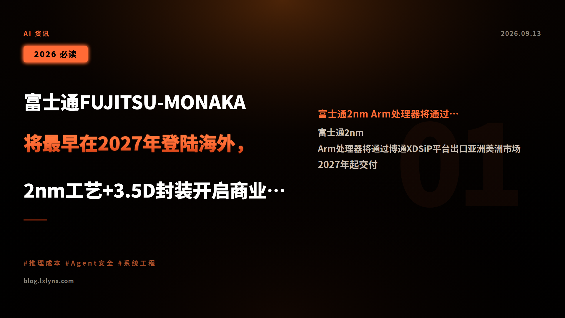
Fujitsu has officially confirmed that its in-house developed ARM-based processor, FUJITSU-MONAKA, fabricated on that 2nm node, will earliest be exported to markets outside Japan—including Asia and the Americas—starting no sooner than 2027. Prior iteration A64FX served exclusively as the compute core for the Fugaku supercomputer, while MONAKA is now explicitly positioned as a sellable commercial product. This marks a strategic pivot from proprietary chip to open-market offering.
Key facts:
- Initial delivery: Already shipped (announced Feb 27 2024)
- Commercial export: Earliest 2027 (Asia & Americas)
- Process node: 2nm (leading-edge)
- Instruction set: ARM
- Packaging: 3.5D XDSiP (provided by Broadcom)
- Target deployment: AI servers
- Progress: 40+ companies in negotiation; 24 verified in financial sector
Broadcom’s 3.5D XDSiP Enables New Packaging Paradigm
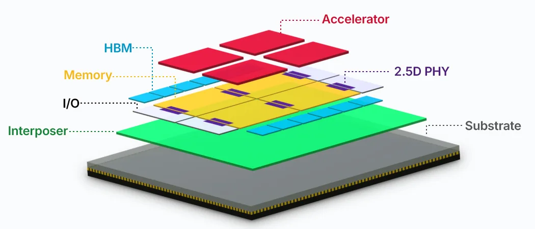
Fujitsu delivers MONAKA using Broadcom’s 3.5D XDSiP advanced packaging platform. 3.5D XDSiP combines 2.5D and 3D-IC techniques, introducing the industry’s first face-to-face (F2F) 3D copper hybrid bonding between top metal layers of stacked dies. This topology shortens interconnect paths, yielding reduced latency, improved power efficiency, enhanced mechanical robustness, and smaller form factors—all critical for dense compute.
Current status shows initial shipments are complete. Broadcom plans additional XPU variants in H2 2026 and projects cumulative sales of over 1 million units by 2027. Surprisingly, while MONAKA is Fujitsu’s silicon IP, its commercial pathway relies heavily on Broadcom as the packaging and delivery partner—highlighting how silicon IP owners increasingly partner with foundry-independent packaging specialists to scale manufacturing.
The counterintuitive insight: A64FX achieved world-leading performance (topping TOP500 in 2020) using only a 12nm node; MONAKA now combines a 2nm process with 3.5D integration, demonstrating that process node leap + advanced packaging yields compounding gains—a more efficient path than reliance on node shrink alone.
From Supercomputer专用 to Commercial read-to-market
Though MONAKA carries the MONA lineage name (Monaka, continuing from A64FX’s project codename), its market role has transformed fundamentally.
| Dimension | A64FX | FUJITSU-MONAKA |
|---|---|---|
| Primary intent | Fugaku supercomputer exclusive | Commercially available product |
| Process | 12nm (TSMC) | 2nm |
| Packaging | Standard 2.5D (silicon interposer) | 3.5D XDSiP (with F2F 3D bonding) |
| Instruction set | Armv8-A | ARM (unspecified generation) |
| Ecosystem | Domestic supercomputing partners | Supermicro (2024), Broadcom (packaging), 40+ AI server vendors |
Fujitsu’s 2024 partnership with Supermicro explicitly positioned MONAKA as a sellable product; negotiations with financial institutions constitute 24 of the 40+ ongoing talks. Market intent has shifted from ‘Fugaku-only’ to ‘AI server first’—leveraging MONAKA’s high-efficiency, low-latency traits for large-model training and inference.
Early adopters vs. wait-and-see
Buyers to monitor:
- AI cloud providers and server OEMs in Asia/Americas
- Financial enterprises with large-scale model workloads (24 institutions already engaged)
- ARM ecosystem integrators seeking non-x86 alternatives
** those to defer**:
- procurement requiring published SPEC or measured power/performance benchmarks (unreleased)
- projects needing 2026 delivery (exports commence 2027; early XDSiP units ship 2026H2)
- existing x86-based deployments (MONAKA requires ARM software stack rework)
Final thought
MONAKA’s overseas rollout exemplifies a new Japanese semiconductor exit strategy: leveraging packaging innovation as the wedge, partnering with global foundry-agnostic players for scalable delivery. As Moore’s Law slows, 先进封装 is emerging as the next performance lever—Friis’ law of packaging, not just physics, now shapes chip competitiveness.